Microprocessor and Microcontroller
How It's Made: Microprocessors Video:
What is a Microcontroller? - Video:
Full Syllabus & Reference Books:-
Text Books:
- 8051 Microcontroller and Embedded Systems using Assembly and C by Mazidi, Mazidi and D.MacKinlay, 2006 Pearson Education Low Price Edition.
- Microprocessor and Microcontroller by R.Theagarajan, Sci Tech Publication, Chennai
- Microprocessor and Microcontroller by R.Theagarajan, Sci Tech Publication, Chennai
- 8051 Microcontroller by Kenneth J.Ayala.
Reference Books:
- Programming customizing the 8051 Microcontroller by Myke Predko, Tata McGraw Hil
Unit 1: Microprocessor and Applications:-
Intel released the 8085, its follow-up to the 8080, in March 1976. It was popular as an embedded controller, finding use in scales and other computerized equipment. The 8085 ran at 5MHz and contained 6,500transistors. It was built on a 3-micron process and incorporated an 8-bit data bus. The microprocessor is the engine of the pc; without them, pcs would not exist. From a technology point of view, a microprocessor is a cpu on a chip. The first one was introduced in 1971, which makes them about 20 years old.
Microprocessor:
Microprocessors are simply a computer processor that has been configured into the design and function of a microchip. Sometimes referred to as a logic chip, this small component functions as the means of executing the command to start booting up a computer. As part of the process, a microprocessor initiates the activation of all the components necessary to allow the computer to be used, such as waking the operating system.
The basic functionality of a microprocessor is all based on the inherent ability to respond to and generate mathematical and logical operations. This function of small computer processors is made possible with the use of registers. Within the registers resides all the data required by the microprocessor to execute such basic functions as addition and subtraction. The configuration of the registers also allow the microprocessor to handle tasks such as comparing two different numbers, and retrieving numbers from various areas and redistributing them.
At the core of the design for the microprocessor is a series of logical instructions that regulate the order that tasks are received and executed. The presence of the instructions assure that tasks are carried out in a sequence that will flow from the completion of one task and into the logical initiation of the next task in the sequence. For example, when an end user boots up a computer, the first instruction that the microprocessor will execute is the activation of the BIOS, or basic input/output system. From that point, the BIOS will load the operating system into the active memory and move on to the next task in the starting process. Each successive task will be achieved once the previous task is complete.
This is about as simple as a microprocessor gets. This microprocessor has:
- an address bus (that may be 8, 16 or 32 bits wide) that sends an address to memory
- a data bus (that may be 8, 16 or 32 bits wide) that can send data to memory or receive data from memory
- a RD (Read) and WR (Write) line to tell the memory whether it wants to set or get the addressed location
- a clock line that lets a clock pulse sequence the processor
- A reset line that resets the program counter to zero (or whatever) and restarts execution.
Understanding Microprocessors - Video:
External Link:
Evolution Of Microprocessors:-
A microprocessor is the heart, the soul as well as the brain of a computer. In fact, it is a computer in itself. The evolution of the microprocessor has been one of the greatest achievements of our civilization.
The History Of Microprocessors - Video:
External Links:
- www.ami.ac.uk/courses/ami4655_micros/u01/micro01evol.asp
- www.docstoc.com/docs/24482388/History-of-the-Microprocessor
- e-articles.info/e/a/title/The-evolution-of-Microprocessors-from-1971-to-the-Present/
- www.bloggerbaba.com/2011/01/history-of-microprocessor.html
- www.meetingtomorrow.com/cms-category/history-of-the-microprocessor
8085 CPU:-
Intel 8085 microprocessor is the next generation of Intel 8080 CPU family. In addition to being faster than the 8080, the 8085 had the following enhancements:
- Intel 8085 had single 5 Volt power supply.
- Clock oscillator and system controller were integrated on the chip.
- The CPU included serial I/O port.
- Two new instructions were added to 8085 instruction set.
The CPU also included a few undocumented instructions. These instructions were supposed to be a part of the CPU instruction set, but at the last moment they were left undocumented because they were not compatible with forthcoming Intel 8086.
8085 - Video:
External Links:
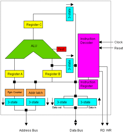
Diagram of 8085 Architecture:

It consists of various functional blocks:
Control Unit:
Generates signals within uP to carry out the instruction, which has been decoded. In reality causes certain connections between blocks of the uP to be opened or closed, so that data goes where it is required, and so that ALU operations occur.
Arithmetic Logic Unit:
The ALU performs the actual numerical and logic operation such as ‘add’, ‘subtract’, ‘AND’, ‘OR’, etc. Uses data from memory and from Accumulator to perform arithmetic. Always stores result of operation in Accumulator.
Registers:
The 8085/8080A-programming model includes six registers, one accumulator, and one flag register, as shown in Figure. In addition, it has two 16-bit registers: the stack pointer and the program counter. They are described briefly as follows.
The 8085/8080A has six general-purpose registers to store 8-bit data; these are identified as B,C,D,E,H, and L as shown in the figure. They can be combined as register pairs - BC, DE, and HL - to perform some 16-bit operations. The programmer can use these registers to store or copy data into the registers by using data copy instructions.
Accumalator:
The accumulator is an 8-bit register that is a part of arithmetic/logic unit (ALU). This register is used to store 8-bit data and to perform arithmetic and logical operations. The result of an operation is stored in the accumulator. The accumulator is also identified as register A.
Flags:
The ALU includes five flip-flops, which are set or reset after an operation according to data conditions of the result in the accumulator and other registers. They are called Zero(Z), Carry (CY), Sign (S), Parity (P), and Auxiliary Carry (AC) flags; they are listed in the Table and their bit positions in the flag register are shown in the Figure below. The most commonly used flags are Zero, Carry, and Sign. The microprocessor uses these flags to test data conditions.
For example, after an addition of two numbers, if the sum in the accumulator id larger than eight bits, the flip-flop uses to indicate a carry -- called the Carry flag (CY) -- is set to one. When an arithmetic operation results in zero, the flip-flop called the Zero(Z) flag is set to one. The first Figure shows an 8-bit register, called the flag register, adjacent to the accumulator. However, it is not used as a register; five bit positions out of eight are used to store the outputs of the five flip-flops. The flags are stored in the 8-bit register so that the programmer can examine these flags (data conditions) by accessing the register through an instruction.
These flags have critical importance in the decision-making process of the microprocessor.
The conditions (set or reset) of the flags are tested through the software instructions.
The conditions (set or reset) of the flags are tested through the software instructions.
For example, the instruction JC (Jump on Carry) is implemented to change the sequence of a program when CY flag is set. The thorough understanding of flag is essential in writing assembly language programs.
Program Counter(PC):
This 16-bit register deals with sequencing the execution of instructions. This register is a memory pointer. Memory locations have 16-bit addresses, and that is why this is a 16-bit register.
The microprocessor uses this register to sequence the execution of the instructions. The function of the program counter is to point to the memory address from which the next byte is to be fetched. When a byte (machine code) is being fetched, the program counter is incremented by one to point to the next memory location
Stack pointer(SP):
The stack pointer is also a 16-bit register used as a memory pointer. It points to a memory location in R/W memory, called the stack. The beginning of the stack is defined by loading 16-bit address in the stack pointer. The stack concept is explained in the chapter "Stack and Subroutines."
Instruction Register/Decoder:
Temporary store for the current instruction of a program. Latest instruction sent here from memory prior to execution. Decoder then takes instruction and ‘decodes’ or interprets the instruction. Decoded instruction then passed to next stage.
Memory address register:
Holds address, received from PC, of next program instruction. Feeds the address bus with addresses of location of the program under execution.
Control Generator:
Generates signals within uP to carry out the instruction which has been decoded. In reality causes certain connections between blocks of the uP to be opened or closed, so that data goes where it is required, and so that ALU operations occur.
Register Selector:
This block controls the use of the register stack in the example. Just a logic circuit which switches between different registers in the set will receive instructions from Control Unit.
General Purpose Register:
uP requires extra registers for versatility. Can be used to store additional data during a program. More complex processors may have a variety of differently named registers.
Block Diagram of 8085 - Video:
Instruction Cycle -:
Instruction cycle:
We have seen that each phase of the instruction cycle can be decomposed into a sequence of elementary micro-operations. In our example, there is one sequence each for the fetch, indirect, and interrupt cycles, and, for the execute cycle, there is one sequence of micro-operations for each opcode.
To complete the picture, we need to tie sequences of micro-operations together, and this is done in Figure 2. We assume a new 2-bit register called the instruction cycle code (ICC). The ICC designates the state of the processor in terms of which portion of the cycle it is in:
00: Fetch
01: Indirect
10: Execute
11: Interrupt

At the end of each of the four cycles, the ICC is set appropriately. The indirect cycle is always followed by the execute cycle. The interrupt cycle is always followed by the fetch cycle (sec Figure 12.4). For both the execute and fetch cycles, the next cycle depends on the state of the system.
Thus, the flowchart of Figure 2 defines the complete sequence of micro-operations, depending only on the instruction sequence and the interrupt pattern. Of course, this is a simplified example. The flowchart for an actual processor would be more complex. In any case, we have reached the point in our discussion in which the operation of the processor is defined as the performance of a sequence of micro-operations. We can now consider how the control unit causes this sequence to occur.
Thus, the flowchart of Figure 2 defines the complete sequence of micro-operations, depending only on the instruction sequence and the interrupt pattern. Of course, this is a simplified example. The flowchart for an actual processor would be more complex. In any case, we have reached the point in our discussion in which the operation of the processor is defined as the performance of a sequence of micro-operations. We can now consider how the control unit causes this sequence to occur.
See also:
Instruction Set
The instruction set or the instruction set architecture (ISA) is the set of basic instructions that a processor understands. The instruction set is a portion of what makes up an architecture. Historically, the first two philosophies to instruction sets were: reduced (RISC) and complex (CISC). The merits and argued performance gains by each philosophy are and have been thoroughly debated.
CISC:
Complex Instruction Set Computer (CISC) is rooted in the history of computing. Originally there were no compilers and programs had to be coded by hand one instruction at a time. To ease programming more and more instructions were added. Many of these instructions are complicated combination instructions such as loops. In general, more complicated or specialized instructions are inefficient in hardware, and in a typically CISC architecture the best performance can be obtained by using only the most simple instructions from the ISA. The most well known/commoditized CISC ISAs are the Motorola 68k and Intel x86 architectures.
RISC:
Reduced Instruction Set Computer (RISC) was realized in the late 1970s by IBM. Researchers discovered that most programs did not take advantage of all the various address modes that could be used with the instructions. By reducing the number of address modes and breaking down multi-cycle instructions into multiple single-cycle instructions several advantages were realized:
- compilers were easier to write (easier to optimize)
- performance is increased for programs that did simple operations
- the clock rate can be increased since the minimum cycle time was determined by the longest running instruction .The most well known/commoditized RISC ISAs are the ARM, MIPS and SPARC architectures.
CISC and RISC - Video:
Interrupts
The processor has 5 interrupts. They are presented below in the order of their priority (from lowest to highest): INTR is maskable 8080A compatible interrupt. When the interrupt occurs the processor fetches from the bus one instruction, usually one of these instructions:
- One of the 8 RST instructions (RST0 - RST7). The processor saves current program counter into stack and branches to memory location N * 8 (where N is a 3-bit number from 0 to 7 supplied with the RST instruction).
- CALL instruction (3 byte instruction). The processor calls the subroutine, address of which is specified in the second and third bytes of the instruction.
RST5.5 is a maskable interrupt. When this interrupt is received the processor saves the contents of the PC register into stack and branches to 2Ch (hexadecimal) address.
RST6.5 is a maskable interrupt. When this interrupt is received the processor saves the contents of the PC register into stack and branches to 34h (hexadecimal) address.
RST7.5 is a maskable interrupt. When this interrupt is received the processor saves the contents of the PC register into stack and branches to 3Ch (hexadecimal) address.
Trap is a non-maskable interrupt. When this interrupt is received the processor saves the contents of the PC register into stack and branches to 24h (hexadecimal) address.
All maskable interrupts can be enabled or disabled using EI and DI instructions. RST 5.5, RST6.5 and RST7.5 interrupts can be enabled or disabled individually using SIM instruction.
Interrupts - Presentation:
Microprocessor:
A microprocessor, as the term has come to be known,is a general-purpose digital computer central processing unit(CPU). Although popularly known as computer on a chip, the microprocessor is in no sense a complete digital computer.
To make a complete microcomputer, one must add memory,usually read only program memory (ROM) and random-access memory(RAM), memory decoders,an oscillator, and a number of input/output (I/O) devices, such as parellel and serial data ports. In addition, special-purpose devices such as interrupt handlers and counters, may be added to relieve the CPU from time consuming counting or timing chores. Equipping the microcomputer with mass storage devices, commonly a floppy and hard disk drives, and I/O peripherals, such as a keyboard and a CRT display ,yields a small computer that can be applied to a range of general purpose software applications.
Microprocessors Video:
Microcontroller:
Microprocessor is a general purpose device. The prime use of a microcontroller is to control the operation of a machine using a fixed program that is stord in ROM and that does not change over the lifetime of the system.
Nowadays, a lot of electrical and electronic devices are controlled by Micro controllers. For example, digital ups systems utilise microcontrollers to control charging of battery, producing AC wave form from DC, trouble shooting etc.
Microprocessor Questions :-
QUESTION BANK
Very short questions
Q1.What is a Microprocessor?
Q2.What is the difference between a Microprocessor and a CPU?
Q3. Define bit,byte,word and Instruction.
Q4. Discuss the function of ALU of 8085.
Q5. List four categories of 8085 Instructions that manipulate data.
Q6. What are the different Addressing Modes in 8085.
Q7.Why is Data Bus Bidirectional?
Q8. Specify four Control Signals commonly used by 8085 MPU.
Q9. What is the function of the Accumulator?
Q10. What are the various Registers of 8085?
Q11. Discuss Machine cycle and State.
Q12. What are the var8ious Status Flags provided in 8085?
Fill in the blanks:
Q13. Microprocessor 8085 is a ------------------ bit processor.
Q14. The Bus carries bits between Micropocessor and ------------------ .
Q15. Microprocessor has -------- number of pins.
Q16. Address bus of 8085 microprocessor is of -------- bits.
Q17. Data bus of 8085 microprocessor is of -------- bits.
Q18. An Instruction has two parts: Opcode and the -------------.
Q19. The method of specifying an Operand is called--------------.
Q20. Examples of 1-byte instruction -------------------------.
Q21. Examples of 2-byte instruction -------------------------.
Q22. Examples of 3-byte instruction -------------------------.
Q23. STA 2500 H takes ------------------ machine cycles.
Q24. LDA 2500 H takes ------------------ machine cycles.
Q25. MOV A,B takes ------------------ machine cycles.
Q26. LXI H 2600 H takes ------------------ machine cycles.
Q27. ADI ,09 takes ------------------ machine cycles.
Q28. IN ,02 takes ------------------ machine cycles.
Q29. There are ------------- addressing modes.
Q30. Discuss the function of HOLD,READY in 8085.
Q31.What is an Interrupt?
Q32. What are various Interrupt lines in 8085?
Q33. Differentiate between microprocessors and microcontroller in one line.
Q34. PUSH PSW means --------------
Q35. POP PSW means -------------
Q36. The function of ALE is ----------------
Q37. Explain what is “Vectored Interrupt”.
Q38. Specify the crystal frequency required fo an 8085 system to operate at
1.1 MHz.
Q39. What is an assembler.
Q40. RAM of 1K* 8 means --------------------
Q41. There are --------------- opcodes in 8085.
Q42. Examples of direct addressing mode is -----------------.
Q43. Examples of indirect addressing mode is -----------------.
Q44. Examples of register addressing mode is -----------------.
Q45. Examples of implicit addressing mode is -----------------.
Q47. Examples of control signals of 8085 ----------------------.
Q48. Give the priority order of interrupts in 8085.
Q49. Data transfer instructions change the status of flags. State true or false.
Q50. CPM R means ------------------
Q51.The CPU of a computer comprises of ------------------.
Q52. Operand is a term used to refer as --------------.
Q53. An 8-bit microprocessor signifies that it has -----------------.
Q54. The address bus width of 64 KB of memory is ----------------.
Q55. DCR register can be used to decrement the contents of ----------------.
Q56. A 3-byte instrction requires ------------- fetch cycles for its execution.
Q57. A 2- byte instrction requires ------------- fetch cycles for its execution.
Q58. A 1-byte instrction requires ------------- fetch cycles for its execution.
Q59. The term cycle stealing is used for ---------------.
Q60. The instruction MOV A,B belongs to ----------------- addressing mode.
Q61. The instruction MVI A,B belongs to ----------------- addressing mode.
Q62. The instruction LXI H, 2000H belongs to ----------------- addressing mode.
Q63. The instruction LDAX D belongs to ----------------- addressing mode.
Q64. What is memory word size required in an 8085 system?
Q65. Move the contents of register A to register B.
Q66. Move the contents of memory location 2000H to the accumulator directly.
Q67. List the sequence of events that occurs when 8085 MPU reads from memory.
Q68. Load the HL pair with the address 2500H.
Q69. Move the data 09H to the B register.
Q70. Specify the two 8085 signals that are used to latch data in an output port.
Q71. Complement the contents of the carry flag.
Q73. Rotate the contents of the accumulator by one bit to the left through carry.
Q74. What are the control signals necessary in the memory-mapped I/O?
Q75. What are various schemes of data transfer from CPU/memory to I/O devices?
Q76. What are different operating modes of 8255?
Q77. In a microprocessor based system, the address signals are sent by -------------.
Q78. In a microprocessor based system, the address bus is ---------------.
Q79. In a microprocessor based system,the data bus is ----------.
Q80. The basic purpose of timing and control unit is ------------------.
Q81.What are I/O ports in 8085?
Q82. TRAP is a maskable interrupt. State true or false.
Q83. Subroutine is defined as -----------------.
Q84. What are Instructions EI,DI in the 8085 Interrupt process?
Q85. List conditional Call and Return instructions.
Q86. Explain the sequence of a program execution when a subroutine is called &
executed.
Q87. What is stack pointer and explain their uses?
Q88. What is Program counter and its uses?
Q90. The clock frequency required for 8085 is -----------.
Q91. Store the contents of accumulator in the memory location 2500H.
Q92. Increment the contents of memory location 2400H by 1.
Q93. What are the major differences between the 8080 and 8085 microprocessor?
Q94. Demonstrate the uses of instructions DAD,PCHL.
Q95. Decrement the contents of the register C by 2.
Q96. Explain the function of Data converters.
Q97. The instruction SPHL signifies -----------.
Q98. Explain the functions of Handshake signals.
Q99. List the elements of 8255A programmable peripheral interface.
Q100. List the operating modes of 8254 timer.
Short questions
Q1. Distinguish between Accumulator-Based and General Purpose Register – Based Microprocessors.
Q2. Mention the differences between 8085 and 8086 Microprocessors.
Q3. Write a program to add two numbers of 8-bit each.
Q4.What are different types of memory?Explain.
Q5. Explain the need to demultiplex the bus AD7-Ado.
Q6. Write a program to count the number of 1’s in a 8-bit number.
Q7. Expain the functions of ALE and IO/M signas in 8085.
Q8. Show the register contents as each of the following instructions is being executed
MVI C, FFH
LXI H, X X 70 H
LXI D, X X70 H
MOV M, C
LDAX D
HLT
Q9.Specify the contents of the accumulator and status of flags when following instructions are executed.
MVI A, B7H
ORA A
Q10.Explain following signals of 8085.
1) NOP
2) HLDA
Q11. Explain the direct addressing modes and indirect addressing modes of
8085 with example.
Q12. Explain the control and status signals of 8085
Q13.Compare synchronous and asynchronous mode of data transfer.
Q14. With the help of SIM instruction format, write the instruction to mask RST 5.5.
Q15. Explain the function of the 16-bit data transfer instruction LXI and of instruction INX and DCX.
Q16. Explain stack and stack pointer.
Q17. Explain the difference between the bus cycle and the machine cycle.
Q18. Expain the RIM and SIM instruction.
Q19. Explain the following instruction:
a) DAA
b) LDA ,16 bit address
c) STA ,16 bit address
Q20. Explain how information is stored and retrieved from stack using PUSH and POP and the stack pointer.
Q21. Explain the following Subroutines:
a) Multiple calling
b) nesting
c) common ending
Q22. Copmpare similarities between PUSH/POP and CALL/RET instructions.
Q23. List the eight steps to initiate and implement the 8085 interrupt.
Q24. What do you mean by polling.
Q25. How many bytes the following instructions of 8085 need?
a) LDA
b) JNZ
c) RAL
d) MVI A
Q26. What do you mean by memory mapping?explain.
Q27.Explain how to connect multiple interrupts with the INTR interrupt line.
Q28. Differentiate between maskable and non maskable interrupts.
Q29. Explain the following instruction:
a) ADD M
b) CMA
c) CMP B
Q30. What are the functions of SID and SOD pins in 8085.
Q31.How are I/O devices addressed in 8085?
Q32. Explain features of the programmable interrupt controller,8259A with its block diagram.
Q35. How to use RIM and SIM instruction for 8085.
Q36. What are hardware interrupts?Discuss TRAP interrupt.
Q37. Write a program to exchange the contents of memory location 2000 H with the contents at memory location 2500 H.
Q38. Write a program to move the contents of memory location 2000H to accumulator.Increment these contents and place then in location 2001H.
Q39. Explain the function of READY signal of 8085
Q40. Set up 8155 timer to generate pulse after a given time delay
Q41. Explain block diagram of the 8279 Keyboard/Display interface and its operations.
Q42.Explain the functions of the 8259A interrupt controller and its operations in fully nested mode.
Q43. Explain the process of DMA and the functions of elements of 8237.
Q44. Explain the basic concepts underlying the successive-approximation A/D converter.
Q45. What ios RIM?Discuss the bit pattern of the accumulator for it.
Q46. Give some examples of 32-bit and 64-bit microprocessors.
Q47. What are the trade-offs between software and hardware approaches in implementing serial I/O?
Q48. Explain the basic circuit of a D/A converter and define the term Resolution.
Q49. Write instructions to initialize the 8279 in a given mode.
Q50.Explain the RS-232C serial I/Ostandard and compare it with RS-422A standard.
Long questions
Q1. Explain the arhitecture of microprocessors 8085.
Q2. Explain the pin diagram of 8085.
Q3. Explain the requirement of a program counter,stack pointer and status flags in the architecture of 8085 microprocessor.
Q4. Explain the memory mapped i/o addressing scheme.
Q5. Draw and explain the timing diagram of memory read cycle.
Q6. Draw and explain the timing diagram of memory write cycle with example.
Q7. Draw and explain the timing diagram of opcode fetch cycle.
Q8.Explain the direct addressing modes and indirect addressing modes of 8085 with example.
Q9. Assume that the accumulator contents data bytes 88 hand instruction MOV C, A 4FH is fetched. List the steps decoding and executing the instruction.
Q10. Discuss how memory chips and I/O devices are interfaced to a microprocessor.
Q11. Draw and explain the internal block diagram for 8155.
Q12. Explain the block diagram of the 8279 Keyboard/Display interface and its operations.
Q13. Draw a timing diagram to interface a 4K ROM and a 2K RAM consecutively with microprocessor 8085, starting with ROM interfacing at address 0000 H. Explain.
Q14. Draw timing diagrams of
1) I/O read
2) memory read
3) fetch
Q15. State addressing modes of the following modes with instruction with justification
1) CMP B
2) JZ address
3) LDAX D
Q16. Discuss various Addressing modes of 8085 with suitable examples.
Q17. What are the various types of Data formats?Explain with examples.
Q18. Explain five interrupt inputs of 8085 with priority.
Q19.What are Hardware and Software Interrrupts?What is ISS?
Q20. Draw a diagram to interface a 6K ROM and a 2K RAM consecutively with microprocessor 8085, starting with ROM interfacing at address 8000 H.
Q21. What is Interrupt ?Explain enabling,disabling and masking of interrupts with examples.How to transfer data using interrupts.
Q22. Expailn how to use an RST instruction to implement a software breakpoint.
Q23. Explain an interrupt process and the difference between a maskable and non-maskable interrupt by using examples.
Q24. Interface a 10 or 12-bit D/A converter with an 8-bit microprocessor.
Q25. Design a circuit to interface an 8-bit D/A conveter with an 8-bit microprocessor and verify the analog output for a digital signal.
Q26. Explain the block diagram of the 8155 I/O section and timer.
Q30.Explain the function of Handshake signals.What is the difference between setting the 8155 I/O ports in ALT 1 and ALT 3.
Q31. Design a five-minute clock(timer using the 8254 and the interrupt technique.
Display minutes and seconds.
Q32. Explain how the 8237 DMA controller transfers 64K bytes of data per channel with eight address lines.
Q33. Specify handshaking signals and their functions if port A of 8255 is set-up as input port in mode 1.
Q34.xplain mode 0 and mode 1 of 8253.
Q35. Write a program to arrange the following numbers in the descending order- 23H,45H,09H,FFH,08H,27H.
Q36. Explain terms synchronous,baud rate,parity,half and full duplex transmission.
Q37. Explain how data bits are transmitted in the asynchronous format,and calculate the the delay required between two successive bits for a given baud.
Q38. Explain the block diagram and the functions of each block of the 8251 USART (Programmable Communication Interface).
Q39.Write a short note on the following:
a) machine cycle
b) instruction cycle
c) execute cycle
d) Vectored interrupt
Q 40. Interface a 8K RAM consecutively with microprocessor 8085, starting with ROM interfacing at address 8000 H.
Q41. Write a program for a Zero-to –Nine couter.Also draw the flowchart.
Q42. Write a program to arrange the following numbers in the ascending order- 23H,45H,09H,FFH,08H,27H.
Q43. Explain the bus architecture of 8085.
Q44. Define Addresing modes,Data formats with examples.
Q45. What you mean by the power of a Microprocessor? Mention the Architectural Parameters to distinguish between Microprocessors.
Q46. Describe a scheme to demultiplex the multiplexed AD0-AD7 bus of 8085CPU.
Q47. Set up the 8255 I/O ports in the simple I/O and Bit Set/Reset(BSR) mode.
Q48. Write a program to divide the two numbers .
Q49. Explain . the process of the Direct Memory Acess(DMA) and the functions of various elements of the 8237.
Q50. Expain the procedure of interfacing the temperature monitoring system with 8085.
External links:
- www.sjbit.ac.in/qbank/undone/computer%20and%20information%20Science/4sem/mupi.htm
- www.kingsindia.net/QUEST%20BANK/it/EVEN%20SEM/2YEAR/Microprocessor%20QBANK.pdf- PDF
- nptel.iitm.ac.in/courses/Webcourse-contents/IISc-BANG/Microprocessors%20and%20Microcontrollers/pdf/Question_Bank/QBm1.pdf-PDF
- www.rajalakshmi.com/Department/EEE/2008ES/EC1362-QB.pdf - PDF
Pin Diagram of 8085 Microprocessor:-
The below Picture describes the Pin Diagram of 8085 microprocessor

Pin Diagram of 8085 - Video:
The Program Status Word
The PSW register is addressable via SFR address $D0, which is also bit addressable. The SB-Assembler does not automatically assign the name PSW or any bit names it contains. All the names can be assigned using normal labels. A bit address is simply the sum of the base address $D0 and the bit number. E.g. the bit address of CY is $D0 + 7 = $D7
The PSW contains 8 system flags:
| CY | AC | F0 | RS1 | RS0 | OV | F1 | P |
| CY | PSW.7 | Carry Flag |
| AC | PSW.6 | Auxiliry Carry Flag |
| F0 | PSW.5 | Flag 0 available to the user for general purpose |
| RS1 | PSW.4 | Register Bank Selector bit 1(see note) |
| RS0 | PSW.3 | Register Bank selector bit 0(see note) |
| OV | PSW.2 | Overflow Flag |
| F1 | PSW.1 | Flag F1 available to the user for general pupose |
| P | PSW.0 | Parity flag. Set/Cleared by hardware each instruction cycle to indicate an odd/even number of "1" bits in the accumulater |
Note:
The value presnted by RS0 and RS1 selects the corresponding register bank.
| RS1 | RS0 | REGISTER BANK | ADDRESS |
| 0 | 0 | 0 | 00H-07H |
| 0 | 1 | 1 | 08H-OFH |
| 1 | 0 | 2 | 10H-17H |
| 1 | 1 | 3 | 18H-1FH |
8085 instruction set consists of the following instructions:
- Data moving instructions.
- Arithmetic - add, subtract, increment and decrement.
- Logic - AND, OR, XOR and rotate.
- Control transfer - conditional, unconditional, call subroutine, return from subroutine and restarts.
- Input/Output instructions.
- Other - setting/clearing flag bits, enabling/disabling interrupts, stack operations, etc.
Instruction of 8085 - Presentation:
Types of Instruction Presentation:
Data movement instructions-:
Data movement instructions move data from one location to another. The source and destination locations are determined by the addressing modes, and can be registers or memory. Some processors have different instructions for loading registers and storing to memory, while other processors have a single instruction with flexible addressing modes. Data movement instructions generally have the greatest options for addressing modes. Data movement instructions typically come in a variety of sizes. Data movement instructions destroy the previous contents of the destination. Data movement instructions typically set and clear processor flags. When the destination is a register and the data is smaller than the full register size, the data might be placed only in the low order bits (leaving high order bits unchanged), or might be zero- or sign-extended to fill the entire register (some processors only use one choice, others permit the programmer to choose how this is handled). Register to register operations can usually have the same source and destination register.
Mov Instruction:
MOV (Move) transfers a byte, word, or doubleword from the source operand to the destination operand. The MOV instruction is useful for transferring data along any of these paths There are also variants of MOV that operate on segment registers
The MOV instruction cannot move from memory to memory or from segment register to segment register are not allowed. Memory-to-memory moves can be performed, however, by the string move instruction MOVS.
XCHG (Exchange) swaps the contents of two operands. This instruction takes the place of three MOV instructions. It does not require a temporary location to save the contents of one operand while load the other is being loaded. XCHG is especially useful for implementing semaphores or similar data structures for process synchronization.
The XCHG instruction can swap two byte operands, two word operands, or two doubleword operands. The operands for the XCHG instruction may be two register operands, or a register operand with a memory operand. When used with a memory operand, XCHG automatically activates the LOCK signal.
No comments:
Post a Comment